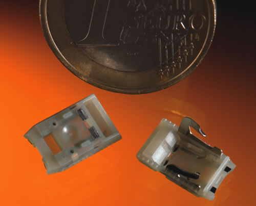
MICRO MOLDING FOR MICRO-ELECTRONICS
Perhaps like no other, the field of microelectronics exemplifies the drive towards miniaturization, the obvious reduction in size of everyday household appliances and cell phones showing the extent to which products containing electronic components have been reduced in size.

The opportunities that exist for OEMs to ride the wave of the “next big thing” in microelectronics are huge, and in order to fully realize this potential, it is important to engage a micro manufacturing partner that can not only assist in the design of smaller electronic components, but which is also aware of the particular contingencies and issues that apply when manufacturing such components.
Opportunities exist to make smaller and lighter parts, to add micro features to existing parts, or even to add new micro features to micro parts. Accumold has over 35-years experience working with OEMs as they mold complex micro-sized electronic components, and has the expertise to work at early stage design development all the way through to volume manufacture in order to exploit commercial opportunities.
THE MICRO ELECTRONICS SECTOR
Microelectronics is a subset of electronics, but is concerned primarily with the manufacture of extremely small components and integrated circuits, typically in the micrometer scale and smaller. The pressure on design engineers in the microelectronics field today is always to deliver faster, smaller, and more cost-effective solutions while at the same time addressing the impact of intrinsic circuit properties (such as interconnections at the micro scale) — so-called “parasitic” effects. As microelectronics are used in some critical computer and medical devices, all development work must also always have as a priority absolute reliability.
Today, it is estimated that microelectronics is the key enabling technology in over half of all new technical innovations, and today they are found in pretty much every electronic product from cars to buildings, computers, surgical tools and imaging technologies, musical devices, video and wireless communications technologies, and cell phones. Consumer and corporate demand across all sectors will continue to accelerate the growth in microelectronics.
And the future is set fair as well. The Internet of Things (IoT), and such innovations as the “connected car” and smart buildings will all be underpinned by massive development in the area of microelectronics. Advances in integrated circuits, power management, and displays are vital for the continued growth of these sectors.
MICROELECTRONICS — PACKAGING AND MOLDING ISSUES
Beyond the actual design and manufacture of micro-electronic components, there is invariably the issue of electronic “packaging”, i.e. the enclosures and/or protective features built into the product itself (be it a component or an end-use device). Such encapsulants protect semiconductor devices and interconnects from environmental factors such as moisture, corrosion-inducing contaminants, and UV radiation. They also protect the parts from mechanically-induced damage such as bending, vibration, and material fatigue caused by thermal shock and temperature cycling during actual-life applications.
While there are a number of packaging technologies available, one of the most often used is plastic molding which has significant advantages in respect of piece part costs, tooling costs, mechanical and electrical properties, and ease of assembly. A plastic-encapsulated microelectronics (PEM) component consists of an integrated circuit chip physically attached to a lead frame, electrically interconnected to input-output leads, and molded in plastic that is in direct contact with the chip, lead frame, and interconnects.
Typically, PEMs are used in commercial, automotive, industrial, and telecommunications electronics, and consequently there is huge demand. There are massive advantages in weight, cost, size, performance and availability when compared to alternative materials such as glass and ceramics, and so saying, plastic packages have attracted almost total dominance in the microelectronics sector. Today, high quality, high-reliability, high-performance, and low-cost plastic encapsulated microcircuits are common-place, and they are seen as the most cost-effective options for a wide range of microelectronic applications.
Much of this massive uptake has been fuelled by improvements in the fabrication of PEMs which have overcome earlier issues of lack of reliability. These developments included increased purity of epoxy molding compounds; material attributes such as enhanced CTE, glass transition temperature, fracture toughness, moisture desorption, adhesion, viscosity, mold release, and appearance; lead frame design; die design and coatings; fabrication equipment; and testing procedures. This has had a massive impact on failure rates, which have reduced from about 100 per million devices from the 1970s to pretty much zero today.
What is extremely obvious when looking at developments in PEMs, is that it is vital that microelectronic OEMs and micro molding agencies partner on product development , as many of the advances on the packaging side can influence product design.
Packaging will actually alter electronic designs and layout on semiconductor chips, circuits, and systems. Recent findings suggest that cost is today the leading factor in nearly all microelectronic packaging applications, and together with increased density of elements on the chip is the main reason dictating ultimate package selection. Cost is also driving the outsourcing of packaging, which helps to optimize manufacturing cycle times, reduce working capital, and improve quality.
Accumold has been the sub-contractor of choice for countless microelectronic projects over the last 35 years. Handling, inserting, or assembling micron-sized parts during manufacture can be an issue. Labor-intensive manual handling is expensive and can damage or contaminate parts. Robotics may not have small enough actuators. Accumold’s tooling and automation systems for lead frame molded parts and insert applications are second to none. Using Accumold's unique technology, the company can mold plastic on and around different types of metal, plastic, fabric or other materials. Some of these processes produce completed parts while others are ready for further processing by the customer.
Manufacturing lead-frame molded parts requires the fabrication of a system to feed the metal lead frame into a machine and extract the complete component from the metal after the plastic has been molded to it. Accumold’s team are expert at fabricating a trouble-free and efficient system to mold the most complex and sophisticated lead frame molded parts.
Accumold is also expert at insert molding, where an existing or previously manufactured part is molded in and around a wide variety of materials from metals to glass and other plastics. This means that in the area of microelectronics, the company can present a portfolio of services that extend into numerous microelectronic applications such as flex-circuit overmolding, and the manufacture of small mold housings, lead frame bobbins, molded lead frame rotors, molded micro-rotors, PEEK lead frame switches, and open cavity packaging.
In addition, Accumold is expert in the process of reel-to-reel micro molding or “strip molding”, which allows the manufacture of small combination metal and plastic parts automatically, rather than having to resort to individual, costly, time-consuming, and inefficient assembly. Reel-to-reel micro molding ensures cost-effective part assembly with consistent alignment and orientation of parts.
SUMMARY
Microelectronics are often used in critical applications, and the ability to be able to manufacture them reliably, cost-effectively, and in volume is vital for the success of many OEM product development projects. The collision of new micro fabrication technologies, new micro molding technologies and materials, and new developments that are facilitating the production of smaller and smaller electronic components open up huge areas for innovation. It is important that microelectronic OEMs engage and work with expert micro manufacturing partners such as Accumold to take advantage of their knowledge of Design for Micro Molding (DfMM), and to take advantage of the array of possibilities that are available through the correct applications of micro manufacturing and micro molding technologies.
www.accu-mold.com
Aaron Johnson is the VP of Marketing and Customer Strategy at Accumold. The company has grown to a 130,000 square foot fortified facility designed for assurance of supply, employs over 350 staff, and is a net exporter shipping all over the world every day from its Ankeny, IA, USA facility which runs 24 hours a day, 7 days a week.
Comments (0)
This post does not have any comments. Be the first to leave a comment below.
Featured Product

