When looking at metrology, general discussion often revolves around the relative merits of contact or non-contact measurement solutions. There is now a drive across nearly all industries for smaller and more complex components.
 3D Optical Metrology – Versatile Tools for Today’s Advanced Manufacturing

Eric Felkel, Product Manager | Zygo Corporation
For these exacting applications, non-contact optical metrology solutions are typically the best fit with its extreme precision and measurement repeatability – vital characteristics when nanometers can make the difference between pass and fail.
Typically, non-contact optical metrology solutions cause no damage to parts being measured, and are also much faster than contact systems. This is ideal when the requirement is for high sampling rates of complex products. In addition, 3D optical metrology tools may be incorporated “in process”, which is where the future of metrology exists in advanced manufacturing scenarios. Measurement systems are moving from dedicated metrology rooms or the quality control department closer to, or — in some cases — onto the production floor.
It is difficult to argue that any alternative metrology solution is close to 3D optical metrology when it comes to the evaluation of a vast number of data points quickly and with precision. As such, in a world where manufacturers increasingly require greater functionality with minimal cost and effort, 3D optical metrology solutions are critical to competitiveness.
It is true that in some sectors, there is still a reluctance to deploy optical measurement systems, which is based in part on misconceptions about reliability, lack of experience, or because out-dated metrology tools are confused with the next generation optical metrology solutions of today. Recent advances in optics, computers, high resolution sensors, and data processing capabilities make such reservations redundant, and in 2020, optical metrology is standard in industry sectors such as consumer electronics, semiconductor, automotive, medical, and aerospace.
PROCESS CONTROL
For many manufacturers, quality control is key to cost-effective and efficient manufacturing, and sub-standard metrology solutions have real cost implications. Because of this, optimum quality management systems are key to competitive success.
Increasingly, the demand is for automated, non-contact metrology systems as part of a production line where high frequency part inspection is required. In addition, there is a growing emphasis on traceability, increased productivity, and global expansion which necessitates making important production decisions from geographically distributed manufacturing facilities.
Because of these demands, industry requires absolutely precise, accurate metrology on all parts produced. 3D optical metrology solutions provide the ability to fulfil such exacting process control requirements
ZYGO & OPTICAL METROLOGY
50 years ago, ZYGO was founded to provide custom optics and precision engineering systems for optics fabrication. As a natural extension of its optics manufacturing activity, the company soon became synonymous with metrology for positioning and surface analysis, and today about 70% of ZYGO’s business is based on the manufacture of 3D optical profilers, laser interferometers, and nano-position sensors.
ZYGO’s optical metrology instruments exist at the ultra-precise end of the measurement spectrum, aimed specifically at high-value applications in semiconductor lithography, consumer electronics, optical testing, and precision manufacturing. In all these areas, high performance three-dimensional metrology is the key to process development and manufacturing yield.
From ZYGO’s unique perspective, the key demand from users of high-precision metrology tools is for greater data density in ever more complex applications. This metrology is often to be undertaken in extremely difficult environments, where traditional metrology tools would struggle to operate efficiently due to vibration or turbulence. In addition, extracting the maximum data possible from each scan is critical to enabling superior metrology on the widest range of samples.
With this pressure on metrology tool manufacturers to preserve measurement precision and flexibility in challenging environments, ZYGO has developed technologies such as its SureScanTM for vibration robust metrology on its 3D optical profilers. In addition, a host of capabilities such as oversampling, High Dynamic Range scans, and industry leading signal processing techniques give rise to ZYGO’s “MoreDataTM” technologies, which maximize the data quality and capability.
These technologies help to bring the instruments closer to the production floor and facilitate measurement of virtually any surface from the very smooth, to the very rough, and from very flat to highly sloped, stimulating in-process metrology applications.
METROLOGY & SMART PHONE COMPONENTS
One perfect example of industry demand for high accuracy metrology with greater data density is in the manufacture of mobile phones, which has metrology needs across the component spectrum. Applications that include camera modules, flexible circuits, and mechanical components all require critical metrology
Lenses. Camera lenses used in smart phones are made up of aspheric elements. The manufacturing yield for a smart phone lens assembly depends not only on the shape of these complicated aspheres, but on the various built-in features that allow individual lenses to fall into alignment when assembled in a lens barrel.
As cameras increase in image quality, tolerances of lens designs become tighter, and at the same time characterization requirements become broader. Increasingly complex camera designs require complex surface geometries. With approximately 40 million micro lenses manufactured every day, there is critical demand for fast, high-quality, reliable metrology to support this scale of precision manufacturing.
Lens manufacturers require as much information as possible about the surfaces and the interlocking alignment features quickly and with high confidence. For this application, ZYGO developed its COMPASSTM 3D optical profiler system, which combines interference microscopy, multi-axis staging, and software for evaluating lens molds as well as individual production lenses.
Through full-surface 3D metrology, the COMPASSTM system characterizes these complex surfaces without compromising precision or accuracy, and can identify defects such as deviation from design and process asymmetries or manufacturing errors that would otherwise be missed, and which would be detrimental to lens performance and image quality. Identifying and quantifying defects can give manufacturers valuable insight about their processes. (See Figure 1.)
.jpg)
A typical COMPASS texture map of a full mobile phone camera lens mold pin. One can clearly see the circular tooling marks from the diamond turning as well as the radial waviness arising from small vibrations on the cutting tool when the pin was manufactured.
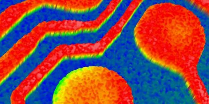
Flexible Circuits. Many of the internal components of a modern smart phone are connected using flexible circuits in order to save space, weight, and energy consumption. These circuits pack a large quantity of connections into a small area, and minor flaws in a relatively small, inexpensive component can result in a completely unusable high-value device.
It is important to evaluate the critical lateral dimensions and topography of the components (usually electrical traces) used in such flexible circuits. Historically this would have been done using two separate metrology systems, but ZYGO optical profilers are able to combine both lateral and vertical metrology tasks into a single, automated solution. This saves time as well as valuable real estate in the factory and enables more efficient workflow. (See Figure 2.)
.jpg)
Flexible circuit microelectronics are inspected to verify proper feature height, width, spacing, and continuity using ZYGO’s ZeGage, NewView, and Nexview optical profilers.
Mechanical Components. Mechanical components such as the barrels that camera lenses are mounted into, or the outer housings that contain all the various parts of a mobile phone also have critical metrology needs that include topography features, lateral dimensions, and surface finish. Surface finish is key for cosmetic parts that need to maintain a consistent look across devices, especially when they may be made in various locations and even by multiple vendors. ZYGO instruments like the NewView 9000, Nexview NX2, and ZeGage Pro optical profilers are deployed into applications of R&D, manufacturing, and quality control to monitor parameters such as these. (See Figure 3.)
.jpg)
CSI measures texture on a variety of materials and surface finishing techniques including (a) polishing, (b) grinding, and (c) diamond turning left to right.
In addition, ZYGO's proprietary Mx™ software — which powers all its optical metrology instruments — provides a full suite of measurement results which would typically require 2 or 3 conventional metrology instruments to replicate. Mx™ powers complete system control and data analysis, including interactive 3D maps, quantitative topography data, intuitive navigation, and built-in statistical process control (SPC) with statistics, control charting, and pass/fail limits.
Having a common platform like Mx™ (made internally by ZYGO) allows applications to be developed in an R&D lab on one platform, then deployed globally on any of the platforms – letting manufacturers select the right equipment and options across their organization.
The rapid growth of advanced manufacturing technology in consumer electronics requires metrology instruments that work at the speed of the industry. ZYGO’s range of optical profiler systems like NewView 9000, Nexview NX2, ZeGage Pro, and COMPASS deliver on this need with the right configuration, capability, performance, and price for any given application. Consumer electronics products will only grow more complex over time, so having a versatile, precise, and powerful surface metrology system available is key to whatever comes next.
SUMMARY
Today, high precision metrology solutions must be sourced carefully to ensure that they represent the best fit for particular industrial applications. Increasingly, the demands of manufacturers are for the reliable measurement of increasingly complex or difficult to measure parts and components, and for an increased number of such applications, non-contact optical metrology solutions are the only viable solutions in terms of accuracy and cost-effective results.
The shift towards in-process automated metrology is also a driver behind the uptake of optical metrology tools, but OEMs need to be aware that not all optical measurement solutions are the same. It is vital that any technology solution provider has the sophisticated hardware and software capabilities to maximize the potential for intelligent and in-depth data acquisition and analysis, and provides metrology tools that can fulfil the sub-nanometer accuracy and repeatability requirements of today’s cutting edge industrial applications.
The content & opinions in this article are the author’s and do not necessarily represent the views of ManufacturingTomorrow
Comments (0)
This post does not have any comments. Be the first to leave a comment below.
Featured Product

